
Active Alignment
Maximizing Optical Coupling Yield with Automated Active Alignment
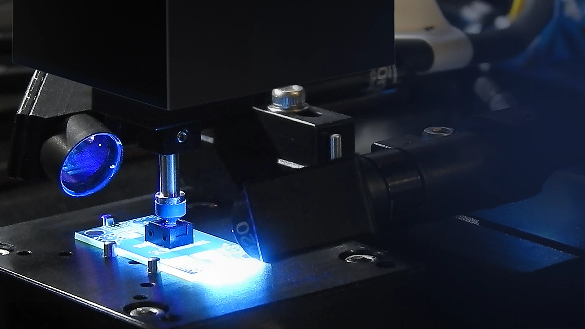
Tresky’s active alignment solutions enable sub-micrometer positioning of fibers, chips, lenses and optoelectronic components using real-time optical feedback. Designed for silicon photonics, optical transceivers, LiDAR, quantum technologies and advanced packaging, Tresky combines high-precision 6-DOF motion with proven DIE bonding expertise to improve coupling efficiency, process stability and production yield. This combination of high-precision DIE bonding, optical feedback integration and flexible photonics assembly in one automation platform guarantees outstanding performance.
Active Alignment for Photonics and Optoelectronic DIE Bonding
Active alignment is a key process in modern photonics assembly. Unlike passive alignment, which relies only on mechanical reference features, active alignment uses real-time optical signal feedback during assembly. This allows components to be positioned at the true optical performance optimum, not just at the geometric center.
For silicon photonics, single-mode fiber coupling, optical transceivers, LiDAR, sensors and hybrid photonic modules, this enables low insertion loss, high coupling stability and reproducible production quality.
Why Tresky for Active Alignment?
- High-precision 6-axis alignment
- Real-time optical signal feedback
- Integration of bonding and alignment in one process
- Support for edge, grating, lens, free-space and array coupling
- Suitable for R&D, process development and scalable production
- Reduced insertion loss and improved coupling stability
- Flexible configuration for different photonic package designs
- High-resolution motion control with nanometer step capability
Talk to our experts about your optical coupling requirements
Edge Coupling
Edge coupling refers to a coupling method in which light is coupled into or out of a photonic chip from the side (via the chip edge). An optical fiber or waveguide is precisely positioned in front of the chip facet so that the light passes directly into the integrated waveguide.
This method is characterized by very high coupling efficiency and low insertion loss. However, it requires extremely precise alignment in the sub-micrometer range, as even the smallest deviations can significantly affect performance. Edge coupling is often used in applications with single-mode fibers and silicon photonics, where maximum signal quality is crucial.
Lensed fiber, lens coupling, and free-space coupling
Lensed Fiber
In lensed fiber, the fiber tip is equipped with an integrated microlens. This focuses or shapes the light beam directly at the fiber's exit surface and enables particularly efficient coupling into small waveguide structures, such as in silicon photonics. Lensed fibers are often used when very small mode fields or high coupling efficiency are required in limited installation space.
Lens Coupling
In lens coupling, the light is focused between the source and the target optics using external lenses, such as spherical, aspheric, or cylindrical lenses. This method allows flexible adaptation to different beam profiles and working distances. It is particularly suitable for hybrid modules or applications that require targeted beam shaping and defined spot sizes.
Free-Space Coupling
Free-space coupling transmits light without direct contact over a free optical path. The beam is guided through space and aligned with the target component using suitable optics. This method offers high design flexibility and is ideal for complex optical systems, such as in sensor, LiDAR, or laboratory applications, but requires very precise alignment.
Grating Coupling (Surface Coupling)
Grating coupling, also known as surface coupling, enables light to be coupled into or out of a waveguide through an integrated diffraction grating on the chip surface. Instead of coupling light laterally through the chip edge, the optical signal is transmitted vertically or at a defined angle via the surface.
This approach is especially well suited to silicon photonics, as it allows wafer-level testing and supports efficient integration into automated assembly and test environments. Its main advantages are easy access from above and excellent automation potential. Depending on the application, trade-offs may include somewhat lower coupling efficiency and narrower bandwidth compared with edge coupling.
Loop Coupling
Loop coupling is a special coupling method in which the optical fiber is guided in a defined loop before being connected to the optical component. This loop guide serves to reduce mechanical stress, compensate for thermal expansion, and ensure stable, low-loss light transmission.
Loop coupling is used particularly in high-precision photonics and sensor applications where long-term stability, vibration resistance, and reproducible coupling efficiency are crucial.
Fiber Coupling
Fiber coupling describes the precise coupling of light between an optical fiber and a photonic or optoelectronic component, such as a chip, laser, or detector. The aim is to transmit as much optical power as possible with minimal loss while ensuring high process stability.
Depending on the application, different concepts such as edge coupling or grating coupling are used. Due to the very small mode fields, especially in single-mode fibers, fiber coupling requires sub-micrometer alignment accuracy and stable, reproducible manufacturing processes.
Array Coupling
Array coupling refers to the simultaneous optical coupling of multiple channels between a fiber array and a photonic chip or module. In this process, multiple fibers, for example in a V-groove array, are aligned parallel to corresponding waveguides or emitters.
The goal is to achieve high-precision, reproducible alignment of all channels with minimal insertion loss and low channel-to-channel variations. Array coupling enables high integration density, scalable bandwidth, and efficient series production, particularly in applications such as parallel transceivers, silicon photonics modules, or high-speed data connections.
Download Product Information
Are you looking for more information? Download further information on active alignment and photonics bonding today.
Photonics Bonder
Active Alignment
Learn more about Active Alignment by Tresky – contact us now.
Contact:
Tresky GmbH
Neuendorfstrasse 18 B
16761 Hennigsdorf
Germany
Tel.: +49 3302 86692-0
Email: info@tresky.de
TRESKY GmbH has its headquarters in Hennigsdorf near Berlin, in the middle of a technology park that is home to numerous highly specialized companies in the fields of automation, electrical engineering, communications technology and life sciences.



Tresky GmbH
Neuendorfstraße 18 B
16761 Hennigsdorf
Germany
+49 (0) 3302 866 92-0
info@tresky.de