- Home
- Services
Services
Your solution for prototyping and small series in semiconductor assembly and packaging technology
Looking for a reliable partner for prototypes and production of small to medium quantities? Our Contract Manufacturing Hub offers comprehensive solutions.
Contract Manufacturing Hub
In the prototyping phase, when producing small series or batch size 1, many companies hesitate to invest in their own DIE-Bonder. Often the final design process has not yet been completed, so that downstream changes to the product or even the manufacturing processes are possible.
Nevertheless, there is often a desire to have these prototypes and small series produced as quickly as possible and without any loss of quality. We will gladly take over this service for you! With a great deal of technical know-how and our many years of experience, we can take over the production of prototypes and small series for you from the first piece onwards on our systems.
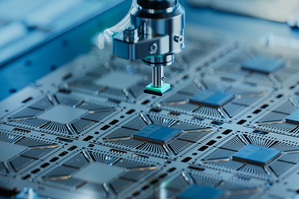
You can access the following processes in our Contract Manufacturing Hub:
- DIE Attach for precise attachment of semiconductor chips
- Eutectic Bonding for robust and durable connections
- Ultrasonic Bonding for efficient connections with high strength
- Sintering for superior material properties through high-temperature processes for power electronics
- Flip Chip Bonding for direct connections for improved electrical performance
- Epoxy Bonding for versatile adhesive connections for various applications
- DIE Sorting for reliable classification and selection of semiconductor chips
This results in significant advantages:
- State-of-the-art technologies for highest precision and reliability
- Customized solutions for your specific requirements
- Fast and efficient implementation of your projects
- Reduction of your development times and time-to-market
- Flexibility because we adapt to your requirements
- Expert support and advice from our experienced team
As an external partner, we can quickly produce small batches on demand without you having to build up production capacities, use existing resources or even interrupt series production.
Optimize your production costs and times without compromising on quality. Contact us today and start your next project with our Contract Manufacturing Hub!
DIE Sorting up to 12“ Wafer,
Pick & Place and Packaging
Packaging semiconductor DIEs in Gel Packs, waffle packs, trays or tapes is essential for protecting these sensitive components during handling and transportation. Each packaging method offers unique benefits in terms of cushioning, automation compatibility, and storage efficiency. Gel Packs are known for their effective cushioning properties, waffle packs are ideal for automated handling, trays provide organized storage, and tape & reel is great for transporting dies in bulk. It’s important to choose the right packaging method based on the specific requirements of your semiconductor components to ensure their safety and protection.
DIE Sorting
| Input | Wafer (4”/6”/8”/12”) Tray (Jedec, Custom) Tape & Reel |
| Output | Waffle Pack / Gel-Pak® (2”/4”) Tape & Reel (Heat Seal) Wafer (4”/6”/8”/12”) Tray (Jedec, Custom) |
| Options | Wafer mapping Inked DIE DIE flipping 180° |
Process Development
We provide process development for various bonding technologies from manual production to semi-automated or fully automated production solution.
Process know-how is the key to achieve the shortest time to market for your product. Our Application Engineers are having specialist knowledge to support you with the best solution.