Vertical Integration of Chips for Compact Components
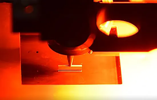
3D bonding is an assembly process in which multiple chips are stacked on top of each other on a substrate. Tresky’s 3D bonders enable this vertical integration as well as a compact arrangement of different circuits with different dimensions in a very small area. DIE stacking is gaining higher importance because it offers a way to overcome the limitations of traditional scaling in the semiconductor industry. It is already a key technology for building 3D NAND flash memories and heterogeneous integration.
The Potential of 3D Bonding in Electronics Devolpment
3D bonding, also called DIE stacking, is an approach in microelectronics and microsystems engineering in which multiple semiconductor chips or components are stacked vertically and bonded together to increase the performance, functionality and density of electronic assemblies. This technology allows multiple layers of chips to be integrated into a single assembly package, rather than arranged side-by-side on a flat surface.
Added Values
More Compact Design
3D bonding allows multiple chips to be placed in a vertical stack, significantly reducing the space required on the PCB or substrate. This is especially beneficial in applications where space is limited.
Short Signal Paths
Because the chips are close together in a 3D stack, the connecting paths for signals and data are very short, which improves signal integrity and can increase transmission speeds.
Improved Performance
By integrating different chips with different functions in a stack, 3D integrations can increase the overall performance and functionality of an assembly. This enables the development of more powerful and versatile electronic devices.
Lower Energy Dissipation
Shorter signal paths and the ability to implement efficient thermal solutions help reduce power consumption and extend battery life in mobile devices.
Improved Thermal Performance
By arranging chips in a stack, heat sources and cooling components can be made more efficient, improving thermal performance and reliability.
Integration of Different Technologies
3D integration enables the combination of multiple technologies, including MEMS (microsystems), sensors, logic chips, communication chips and more, into a single assembly.
Heterogeneous Integration
It is possible to integrate chips from different manufacturers and technologies in a 3D stack, which is called heterogeneous integration. This opens up new opportunities for innovative products.
Scalability
3D Bonding can be adapted for a wide range of applications and integration requirements and is therefore scalable.
Variable Parameters DIE Stacking
- Number of chips in vertical view