Reliable Direct Connection of Chips on a Substrate
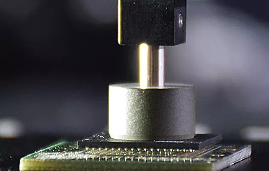
Flip chip bonding is also known as C4-technology (Controlled Collapse Chip Connection). This is a process of assembly and connection technology for contacting unpackaged semiconductor chips, so-called bare DIEs by means of bumps. Tresky’s Flip Chip bonder enables this precise and sensitive DIE bonding process.
Increased Efficiency through Direct Chip Assembly and Maximum Contact Density
In flip chip assembly, the chip is mounted directly to the substrate/circuit carrier with the active contact side facing down, without any further connecting wires. This is where the name flip chip comes from. By mounting the chip directly on the substrate or circuit carrier without additional connecting wires, not only package dimensions are downsized, but conductor lengths are also reduced, allowing more efficient interconnection. For very complex circuits, this technology often offers the only reasonable connection option, because in some cases several thousand contacts have to be implemented. In this way, the entire area of the DIE can be used for contacting.
With Tresky’s flip chip bonders, high packing densities that require less space can be reliably implemented. At the same time, flip chip bonding enables shorter signal paths and higher frequencies. Furthermore, with the flip chip bonding technique, all contacts are connected simultaneously, reducing cycle times.
Added Values
High Connection Density
In flip chip bonding, the connection points are applied directly to the chip surface and connected to the contact pads on the substrate or PCB. This enables a very high interconnect density, as no wire connections are required as with other assembly techniques, e.g. wire bonding
Short Signal Paths
Since the connection points are placed directly over the chips, the signal paths are very short. This reduces electrical losses and enables faster signal transmission, which is especially important in high-speed applications.
Improved Thermal Performance
Direct contact between the chip and the substrate enables efficient heat transfer. This is critical for cooling high-performance chips, as it helps keep operating temperatures low and extends chip life.
Better Mechanical Stability
Flip chip bonding can provide a robust mechanical connection because the chips are placed directly on the substrate and fixed with solder joints or other bonding materials. This makes the assembly more stable overall and less susceptible to vibration and shock loads.
Versatility
Flip chip bonding can be used with a variety of chips and substrates, including semiconductor chips, MEMS (microsystems), optical devices and more. It enables the integration of multiple technologies into one single assembly.
Cost Efficiency
Although the process technology and materials can be specialized, flip chip bonding can be cost effective in mass production because it is faster and more precise than some alternative assembly methods.
Reduced Footprint
Smaller and more compact electronic assemblies can be produced due to the smaller size and space requirements of the interconnect points.
Suitability for Three-Dimensional (3D) Integration
Flip chip bonding is well suited for realizing 3D integration, where multiple chips are stacked on top of each other to increase performance and functionality without increasing space requirements.
Variable Parameters for Flip Chip Bonding
- Bonding force (pressure)
- Temperature
- Bonding time