Events
An overview of our trade fair appearances and events
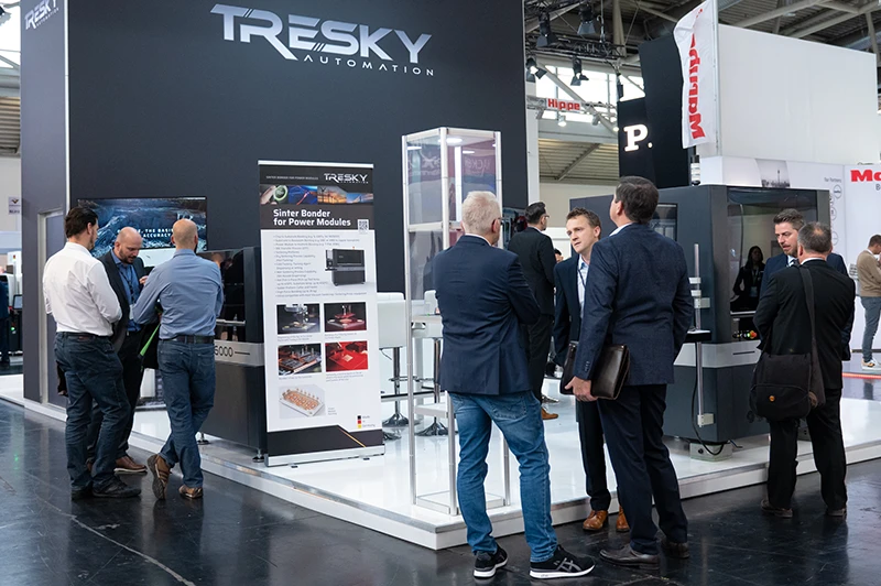
As a leading company in the field of DIE bonding, we regularly take part in global trade fairs and events related to the semiconductor industry to present our latest products and innovations. Please contact us in advance for a personal appointment. Here you will find an overview of our upcoming trade fair participations: