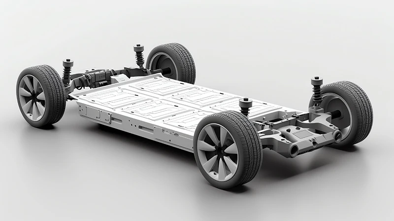
Assembly and Connection Technology for E-mobility Solutions and Power Electronics
For bonding semiconductors such as IGBTs, SiC MOSFETs or GaN HEMTs with Ag on DBC or AMB substrates or for connecting power modules on heat sinks, metallic sintering offers a high-performance assembly and connection technology with maximum reliability. Tresky’s sinter bonders enable the use of copper sinter paste, thixotropic silver paste, and DIE Transfer Film (DTF).
Metallic Sintering
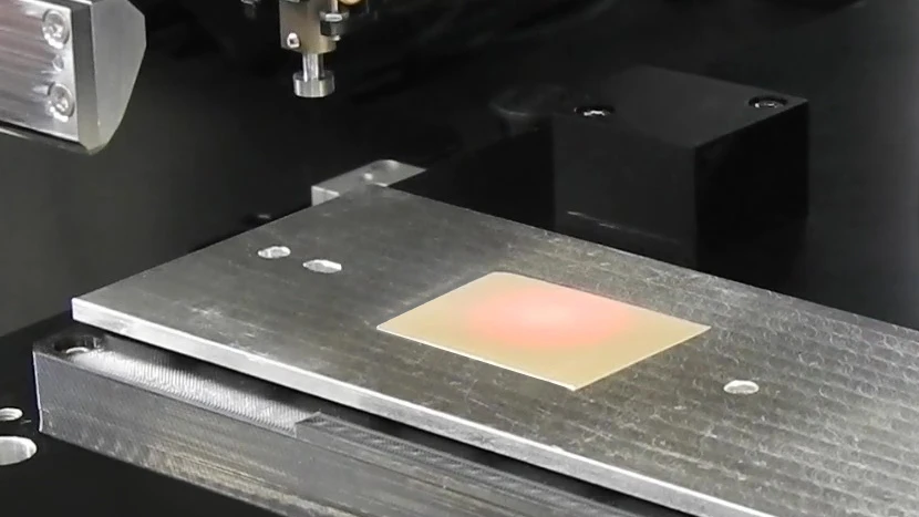
When performing sintering, the chip is bonded to a substrate using sintering paste with the aid of heat and pressure. Typically, copper or silver sintering pastes are used. During the actual sintering process, the metal particles are bonded together by diffusion processes. The advantage over soldering processes is better thermal conductivity, longer service life and high thermomechanical stability. These properties are particularly important in electromobility and power electronics.
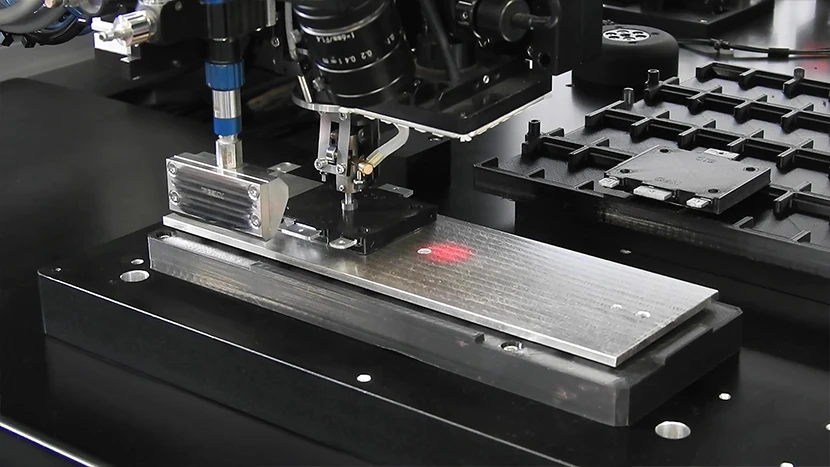
Precise application of the paste is the first step for a reliable, reproducible pre-sintering process in assembly and connection technology. For this purpose, Tresky uses the SQ-Nozzle developed for this purpose, which ensures a very homogeneous and large-area application of paste. The repeatability of the defined layer height or thickness is validated by an optical measurement system. After application of the sintering paste, the power semiconductor is placed within the machine in a second process step.
Flyer Sintering Bonder PDF
White Paper: Motivation for Sintering in Semiconductor PDF
Sintering with the DTF Process
During the DIE transfer film process, a thin silver sinter layer, a so-called transfer film, is first picked up with the DIE. The picked chip is pressed into the film with a defined force and temperature. When the component is subsequently lifted, a uniformly thick, defined layer is released from the film. Due to the good adhesion the layer remains adhered to the underside of the chip. The chip coated in this way is then placed on the Ag or Au pad of the DBC or AMB substrate and fed into the sintering process. After sintering, a high-purity bond is formed between the component and the surface, which exhibits excellent thermal and electrical conductivity.

Large Area Sintern
Large Area Sintering (Half-Bridge Modules) in Power Electronics
The integration of large-area power modules and half-bridge modules with an area of over 100 mm² is highly relevant. These modules are of great importance for various applications in e-mobility, as they offer high power density and efficiency.
Tresky allows dispensing of over 100 mm² for large area sintering applications
However, connecting these components is challenging. Bonding of components, AMB substrates, or PCBs used with heat sinks using silver sintering become a high technical challenge. Factors such as warpage, surface quality, and the application and processing of pastes become increasingly complex. In particular, problems arise during the dry sintering process for large power semiconductor modules, such as the difficult printability of large areas with the paste printer, the formation of depressions, also known as cavities, and warping on the AMB substrates or modules themselves. Air pockets (voids) can form between the substrate and power module, affecting the connection and potentially leading to microcracks.
Reproducible wet sintering process
The wet sintering process offers a promising alternative. In this process, the wet sinter paste is applied to the substrate on a large area using a dispensing method, and the module or semiconductor is then placed directly into the paste. This method allows for compensating for the warpage of components such as the substrate and semiconductor chip through the wet sinter paste. Minimal layer thicknesses can be achieved through the dispensing process. Large Area Sintering can reduce material consumption and production costs.
Development and optimization of sintering processes
The development and optimization of these specific sintering processes are crucial for producing reliable and efficient large-area power semiconductor modules. Improving connection techniques and reducing defects also increases the modules’ lifespan, leading to higher performance and operational safety, for example, in electric vehicles.
Continuous research and innovation in this area are essential to meet the industry’s increasing demands and drive technological development forward. Advanced sintering processes significantly contribute to competitiveness and sustainability, especially in e-mobility and power electronics, where efficiency and reliability are of central importance.