Platform for Advanced Chip Assembly and Process Development
The Lab Bonder, based on the T-200 machine platform, is a high-precision platform for demanding research and development applications in microelectronics, photonics and precision assembly. Designed for maximum stability and process control, the system delivers reproducible bonding results in the sub-micron range, thereby meeting the most stringent requirements for accuracy and reliability.
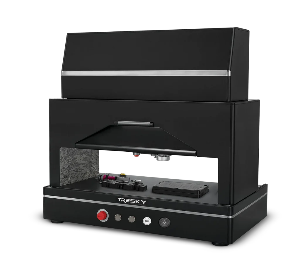
All DIE Bonding Functions in Less Than Half a Square Meter
The Lab Bonder has been specifically designed for research and development environments where the highest precision and process stability are crucial. With a placement accuracy in the sub-micrometer range of ±0.7 μm, the Lab Bonder enables bonding processes with sub-micron accuracy and guarantees exceptional reproducibility, even for complex applications in microelectronics and photonics. This makes the Lab Bonder ideally suited for demanding development projects where the smallest tolerances and the highest precision are crucial to success.
Flyer
Lab Bonder
Flexibility for Prototyping and Validated Processes
A key advantage of the system is its high degree of flexibility. The Lab Bonder supports both manual and fully automated operating modes, thereby covering the entire spectrum from rapid prototyping to stable, reproducible processes for validated research workflows. Engineers and developers benefit from intuitive operation, precise alignment and reliable process performance, which ensures consistent results.
Compact Design with Maximum Precision
Despite its high performance, the Lab Bonder impresses with its extremely compact design. With a footprint of 600 x 750 mm, the system integrates all relevant bonding technologies into a single platform. This allows valuable laboratory space to be utilized efficiently without having to compromise on functionality or productivity. The Lab Bonder also features a direct measurement system in the X and Y directions with a resolution of 0.001 μm.
Technological Versatility for Modern Assembly and DIE Attach
The Lab Bonder covers a wide range of modern bonding processes, thereby offering maximum technological flexibility and a high degree of modularity. These include, for example, DIE attach and flip-chip bonding, sintering processes (Ag and Cu), ultrasonic bonding and eutectic bonding, thermocompression bonding, as well as adhesive bonding using epoxy or UV materials. This diversity makes it possible to implement a wide range of materials, designs and technologies within a single platform, and to develop and optimize processes in a targeted manner.
Robust Construction for Maximum Accuracy
The mechanical basis of the system is a highly stable, solid granite chassis. A linear axis system with a direct measurement system in the X and Y directions and nanometer-level resolution ensures precise positioning and the highest process accuracy. These design features are crucial for reproducible results and reliable process development, particularly in highly sensitive applications.
Optimized For High-Tech Sectors
The Lab Bonder is specifically designed to meet the requirements of modern high-tech industries. Typical areas of application include semiconductor and microelectronics manufacturing, as well as optoelectronic and photonic applications—such as those used in medical technology and in safety-critical applications like defense and the military. For these industries, the system enables precise process development, which is crucial for both prototypes and small-batch production.
High-Performance Specifications for Demanding Processes
With a working area of 200 × 240 mm and substrate sizes of 8 and 12 inches, the Lab Bonder offers sufficient flexibility for a wide variety of applications. The Z-axis allows for 33 mm of travel, while chip rotation of up to 360° ensures maximum freedom of alignment. The bonding force range extends from a delicate 0.01 N up to 350 N (optionally up to 1,000 N), enabling both delicate and high-force processes.
Added Value
Submicron Accuracy
Submicron placement accuracy enables high-precision bonding processes and ensures that even the most demanding applications in microelectronics and photonics can be reliably implemented.
Reproducibility
Thanks to the system’s high stability and precise control, processes can be repeated exactly, which is a crucial prerequisite for reliable research results and high-quality development processes.
Manual and Automatic Modes
The ability to switch between manual operation and fully automated processes enables both rapid prototyping and the development of standardized processes within a single system.
Bonding Technologies
From DIE attach and flip-chip to sintering processes, thermocompression, and bonding technologies, the Lab Bonder covers a wide range of processes and reduces the need for multiple individual systems.
Stability
The solid granite base minimizes vibrations and provides an extremely stable foundation for the process. This is crucial for precise positioning and consistent quality.
Precision
A high-resolution measurement system in the X and Y directions enables precise motion control and helps ensure compliance with the tightest tolerances throughout the entire process.
Modularity
The system can be flexibly adapted to different applications and technologies and scales to meet the demands of development projects and new processes.
Operation
The user-friendly control system reduces training time and allows developers to focus on the process rather than on operating the machine.
Construction Method
With a footprint of less than 0.5 m², the Lab Bonder offers maximum functionality in a minimal amount of space and is ideal for space-constrained R&D environments.
Applications
The Lab Bonder is specifically designed for applications in semiconductor manufacturing, photonics, medical technology, and defense, and meets the requirements of these highly regulated industries.
Variable Parameters for Photonics Bonding
- Bonding force (pressure)
- Temperature
- Bonding time