
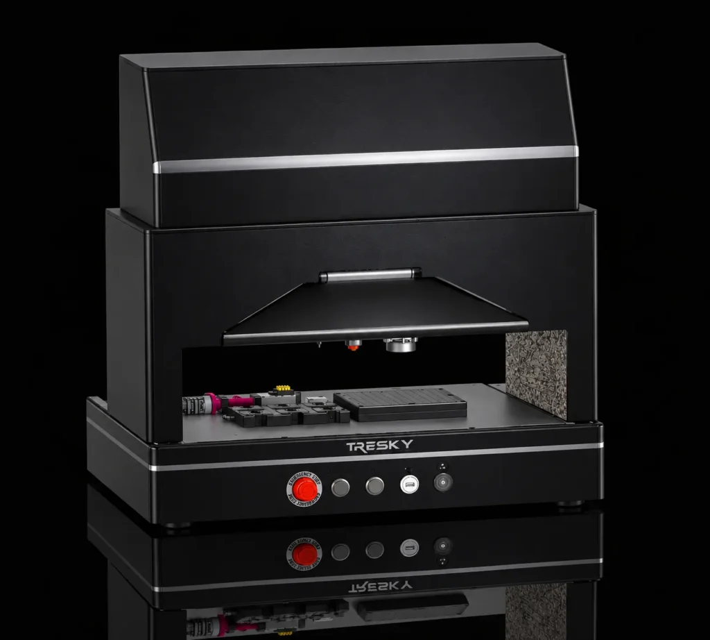
The Tresky GmbH is expanding its portfolio with the new Lab Bonder, based on the new T-200 machine platform. The bonding platform combines submicron accuracy, maximum process flexibility, and a wide range of bonding technologies in a footprint of less than 0.5 m².
The high-precision Lab Bonder was developed specifically for research and development environments and offers a powerful platform for demanding applications in microelectronics, photonics, and modern packaging and bonding technologies. The Lab Bonder supports companies and research institutions in the development and validation of new packaging and bonding processes.
Submicron Precision for Demanding Development Processes
The increasing miniaturization of electronic and photonic systems is challenging product developers even in the development and prototyping phases. Tiny structures, increasing integration densities, and new material combinations require high-precision manufacturing and development platforms. This is exactly where Tresky’s new Lab Bonder steps in. With a placement accuracy of ±0.7 μm, the system enables reproducible bonding processes in the submicron range, paving the way for reliable development and qualification processes.
A key advantage of the Lab Bonder is its flexibility. The system supports both manual and fully automated operating modes. This allows the Lab Bonder to guide users from initial feasibility studies all the way to validated pilot processes on a single platform. Users benefit from the system’s intuitive operation and precise component alignment.
Despite its extensive functionality, the Lab Bonder requires only a footprint of 600 x 750 millimeters. Tresky thus integrates all relevant bonding technologies onto a highly integrated laboratory platform, which saves valuable floor space, particularly in laboratory and cleanroom environments. At the same time, a high-resolution direct measurement system in the X and Y directions, with nanometer resolution, ensures maximum precision with every movement.
Versatile Bonding Technologies on a Single Platform
The Lab Bonder supports a wide range of modern bonding processes. These include, among others, DIE attach, flip-chip bonding, silver and copper sintering processes, ultrasonic bonding, eutectic bonding, thermocompression bonding, and adhesive bonding using epoxy and UV materials. This technological diversity enables users to develop, optimize, and qualify a wide variety of materials and packaging concepts within a single system.
Stable Machine Architecture for Reproducible Results
The basis for this high precision is a solid, full granite chassis that minimizes vibrations and creates an exceptionally stable processing environment. Combined with the linear axis system and the direct measurement system, this provides ideal conditions for reproducible results, even in highly sensitive applications and with the tightest tolerances. With a working area of 200 x 240 millimeters, support for substrates up to 12 inches, such as those used in D2W applications, and a bonding force range of 0.01 to 350 newtons (optionally up to 1,000 newtons), the system covers a wide range of applications. The free chip rotation of up to 360 degrees also ensures high flexibility in the precise alignment of complex components.
Wide Range of Applications in Research and Industry
The new Lab Bonder is designed specifically for companies and research institutions in the fields of semiconductor manufacturing, microelectronics, photonics, optoelectronics, and medical technology. Safety-critical applications in defense, aerospace, and aviation also benefit from the system’s high level of process control and reproducibility.
“With the new Lab Bonder, we offer developers and research teams a platform that combines the highest precision, maximum flexibility, and state-of-the-art bonding technologies in a compact system. This creates optimal conditions for the development of the next generation of electronic and photonic systems.”
explains Daniel Schultze, Managing Director of Tresky GmbH in Germany
Interested in the New Lab Bonder?
Learn more about the applications of the new Lab Bonder and its wide range of bonding technologies. Contact us for a personal consultation tailored to your specific requirements.