
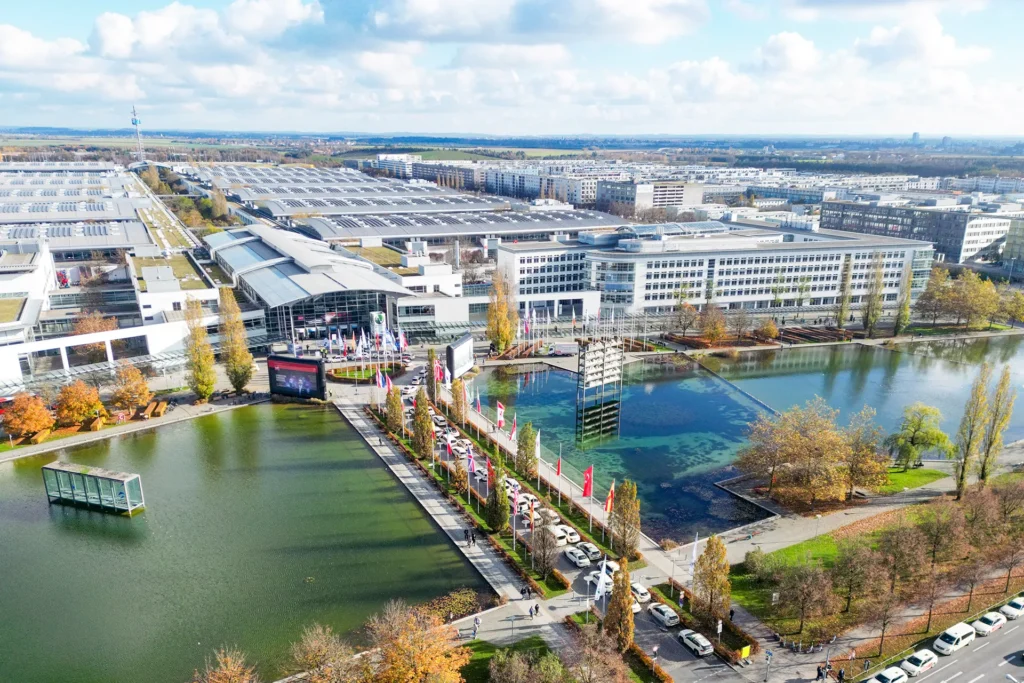
Tresky GmbH will present solutions for demanding AVT and bonding processes in the semiconductor industry at SEMICON Europe 2026, taking place November 10–13 in Munich. The focus of the company’s exhibition will be on active alignment for photonic and optoelectronic components, the software-based Digital Beamsplitter, and the compact T-200 Lab Bonder. These technologies demonstrate how high positioning accuracy, flexible process control, and various bonding technologies can be combined for advanced packaging and heterogeneous integration.
With chiplet architecture and the heterogeneous integration of different semiconductors, materials, and optical components, the demands on assembly and connection technology are increasing. Even slight deviations in component alignment can affect the electrical or optical properties of a package. At the same time, new processes must initially be investigated in the lab, validated for reproducibility, and then refined for industrial applications. To achieve this, Tresky relies on modular DIE-bonding platforms that combine precise positioning with various bonding processes in a single machine.
Active Alignment: Optical performance instead of relying solely on geometric references
When assembling photonic components, merely aligning them geometrically is often insufficient. What matters most is how efficiently light is transmitted between the fiber, lens, laser diode, or photonic chip. Tresky’s Active Alignment therefore uses real-time optical feedback signals to align the components for the highest possible coupling efficiency.
The Active Alignment module, available for all Tresky machine platforms, enables positioning in six degrees of freedom (6-DOF) with a minimum linear step size of 15 nm. During the alignment process, component tolerances can be taken into account, and the optical signals can be continuously evaluated. Various coupling concepts are supported, including edge coupling, grating coupling, fiber coupling, and array coupling. Applications range from silicon photonics and high-speed optical communication to LiDAR sensors and photonic integrated circuits (PICs). Of particular relevance is the ability to combine optical alignment with the subsequent bonding process on a single, integrated platform.
Digital Beamsplitter: Alignment even with chip structures that will be covered
With the Digital Beamsplitter, Tresky introduces a software-based alternative to traditional optical image superimposition. The up-looking camera captures the chip, while the down-looking camera captures the substrate or the target position. Both views are digitally displayed in a single alignment image. This allows deviations in the X, Y, and theta directions to be immediately detected and corrected.
A key advantage applies to components whose alignment marks are covered after being picked up by the pickup tool: Previously captured chip structures remain available as a stored image reference for overlaying with the current substrate image. This expands the alignment options in cases of limited optical accessibility. Since no additional physical beam splitter is required for digital image superposition, the specific optical and mechanical factors associated with it, such as light division and the effort required for adjustment, are eliminated.
T-200 Lab Bonder: Submicrometer precision in a compact footprint
For research institutions and development departments, Tresky presents the Lab Bonder, based on the T-200 platform. The system is designed for the development, investigation, and optimization of various assembly and bonding processes. With a specified placement accuracy of ±0.7 µm, it is suitable for demanding applications in the submicrometer range. A stable, all-granite chassis, along with direct position measurement systems in the X and Y directions with a resolution of 0.001 µm, ensure precise and reproducible process control.
The machine’s footprint is only 600 × 750 mm, which is approximately 0.45 m². Depending on the equipment and process configuration, the platform supports, for example, DIE attach, flip-chip bonding, silver and copper sintering, ultrasonic and thermocompression bonding, eutectic bonding, and adhesive processes using epoxy or UV materials. Users can switch between manual steps for prototyping and automated processes for repeatable test runs. The Lab Bonder thus offers the ability to evaluate different assembly and bonding technologies in a compact manner on a modular platform.
From process development to industrial application
“Today, the requirements in advanced packaging and photonics go far beyond the precise placement of individual components. What matters most is the interaction between positioning accuracy, process control, and the ability to flexibly process different materials and bonding technologies. With our modular DIE-bonding platforms, we help customers develop and validate new processes and prepare them for industrial applications,”
explains Daniel Schultze, Managing Director of Tresky GmbH.
At SEMICON Europe 2026, at Booth B1721, Tresky will provide information on the applications of Active Alignment, Digital Beamsplitter, and the T-200 Lab Bonder. Trade visitors can discuss their specific requirements for positioning, assembly, and bonding with the company’s specialists.
Meet Tresky at SEMICON Europe 2026!
Visit Tresky at SEMICON Europe 2026 at Booth B1721 and discuss your specific positioning, assembly and bonding requirements with our experts.